The Silicon Photonics Breakthrough: How Light is Rewiring AI Chips
As AI clusters scale to unprecedented sizes, the semiconductor industry is moving away from electrical wires. In 2026, co-packaged optics (CPO) are moving into mass production, integrating light-based data transfer directly onto silicon to shatter the AI power wall.
By Factlen Editorial Team
- Foundry Innovators
- Chipmakers view co-packaged optics as the ultimate validation of 3D advanced packaging.
- AI Infrastructure Architects
- System designers see light as the only way to dismantle the data center power wall.
- Optical Component Suppliers
- Laser and material suppliers emphasize the critical role of specialized light sources.
What's not represented
- · Data Center Cooling Engineers
- · Traditional Copper Cable Manufacturers
Why this matters
The physical limits of copper wiring have threatened to cap the growth of artificial intelligence. By replacing electricity with light directly on the microchip, the tech industry is drastically cutting power consumption and enabling the creation of million-GPU AI factories.
Key points
- The semiconductor industry is hitting a 'power wall' as the energy required to transmit electrical signals over copper limits AI cluster size.
- Co-Packaged Optics (CPO) solves this by integrating silicon photonics directly onto the chip package, using light instead of electrons for data transfer.
- TSMC's COUPE platform enters mass production in 2026, utilizing hybrid bonding to stack electrical and photonic dies with near-zero signal loss.
- Nvidia is launching CPO-based Spectrum-X switches in late 2026, delivering 409.6 Tb/s bandwidth and a 5x improvement in power efficiency.
- The shift is driving massive demand for Indium Phosphide (InP) lasers, reshaping the semiconductor supply chain.
For the last decade, the semiconductor industry’s primary obsession has been shrinking transistors to pack more computational logic onto a single piece of silicon. But as artificial intelligence models scale to unprecedented sizes, the most critical bottleneck in 2026 is no longer computation—it is communication. When an AI training cluster grows from a few thousand to hundreds of thousands of GPUs, the physical act of moving data between those chips becomes a monumental engineering challenge. The industry has hit a "power wall," where the energy required to push electrical signals across copper wires threatens to stall the growth of next-generation AI factories.[8]
The fundamental physics of copper are to blame. As data transmission rates push past 800 gigabits per second, electrical signals suffer severe degradation over even short distances. To compensate for this signal loss, data centers must pump massive amounts of power into the system, generating excess heat that requires even more power to cool. Nvidia CEO Jensen Huang famously noted that the industry should use copper for as long as possible, but the consensus in 2026 is that copper has finally reached its practical limit for high-speed AI interconnects.[3]
Historically, the solution to the distance problem has been pluggable optical transceivers. These are modular boxes sitting at the edge of a server board that convert electrical signals into light for transmission over fiber-optic cables, then convert them back to electricity at the receiving end. While effective for traditional cloud networking, this architecture is failing under the weight of generative AI. A modern pluggable transceiver consumes roughly 30 watts of power just to process a 1.6-terabit signal. In a cluster with tens of thousands of connections, the power draw of the optical modules alone becomes an unsustainable burden.[3][4]

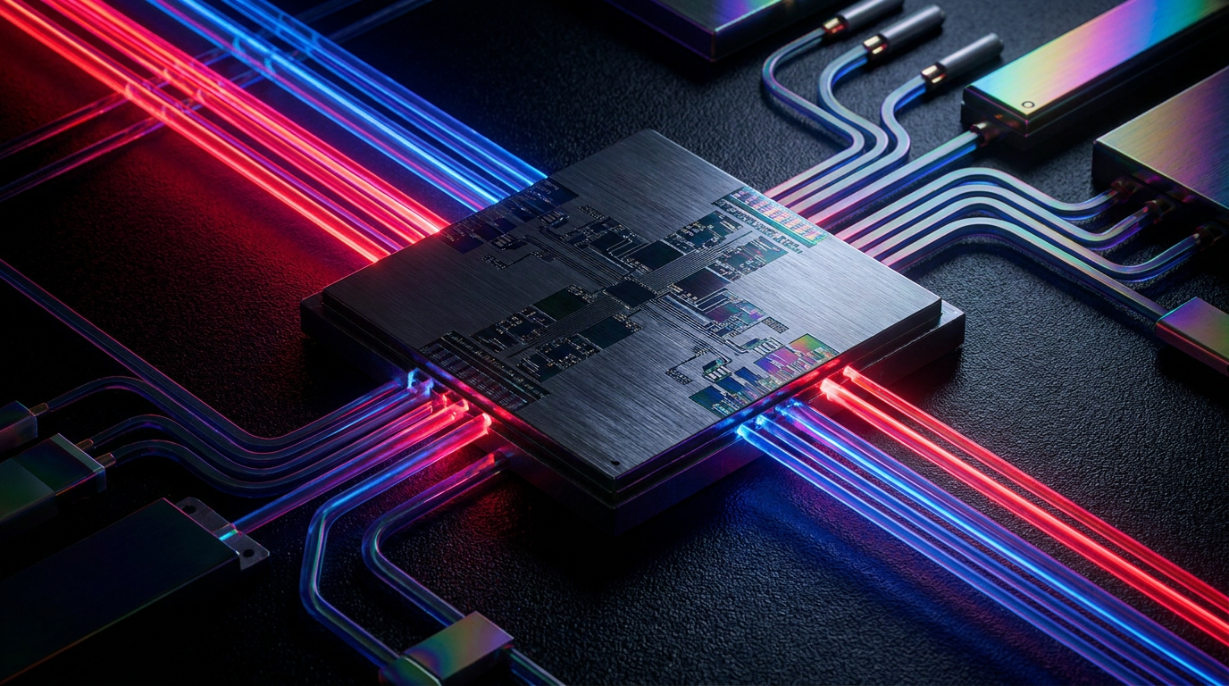
The definitive answer arriving in 2026 is a paradigm shift known as Co-Packaged Optics (CPO), powered by silicon photonics. Instead of relying on discrete pluggable modules at the edge of the board, CPO integrates the optical communication engine directly onto the same substrate as the main networking switch or processor. By moving the light source and modulators mere millimeters away from the logic die, the long, power-hungry electrical traces across the motherboard are entirely eliminated. The chip itself communicates using light.[1][8]
The commercialization of this technology is being spearheaded by the world's largest contract chipmaker. TSMC has officially moved its silicon photonics integration platform, dubbed the Compact Universal Photonic Engine (COUPE), from the research and development phase into full mass production this year. This marks a watershed moment for the semiconductor supply chain, signaling that optical interconnects have achieved the manufacturing maturity required for deployment in hyperscale data centers.[2][4]
TSMC’s COUPE platform is fundamentally a triumph of advanced 3D packaging. Rather than placing the electronic and photonic components side-by-side, COUPE utilizes TSMC’s SoIC-X (System on Integrated Chips) stacking technology. Through a process called hybrid bonding, the electrical control die is permanently fused directly on top of the photonic integrated circuit at room temperature, without the use of traditional metal solder bumps. This microscopic proximity minimizes electrical impedance and signal loss to near-zero levels.[3][4]
The performance gains delivered by this architecture are staggering. According to TSMC's engineering data, the COUPE platform delivers a five-to-tenfold improvement in power efficiency compared to traditional pluggable optics. Furthermore, because the data path and electro-optical conversion process are so drastically shortened, latency is reduced by a factor of 10 to 20. For AI workloads where thousands of GPUs must act synchronously as a single unified system, these microsecond latency reductions translate directly into faster training times and higher hardware utilization.[4]

The performance gains delivered by this architecture are staggering.
The first major beneficiary of this mass-production milestone is Nvidia. The AI chip leader is integrating co-packaged optics into its next-generation networking hardware, launching the Spectrum-X Ethernet Photonics and Quantum-X InfiniBand switches in the second half of 2026. By bringing CPO into the Ethernet ecosystem, Nvidia is ensuring that the cost and interoperability advantages of standard networking protocols can be maintained even at extreme AI scales.[1][5]
Nvidia’s flagship SN6800 switch illustrates the sheer scale of the silicon photonics breakthrough. The quad-ASIC chassis delivers an astonishing 409.6 terabits-per-second of total bandwidth. By replacing traditional transceivers with integrated silicon photonics, the switch achieves a 3.5x improvement in power efficiency and a tenfold increase in network resiliency. Financial analysts tracking the rollout note that this specific architecture is effectively dismantling the power wall that previously capped the maximum size of AI clusters.[5][6]
The transition to light is triggering a massive realignment among foundry giants. While TSMC currently holds the first-mover advantage, Samsung has formally entered the silicon photonics race to prevent a monopoly. Samsung recently unveiled its own roadmap to launch optical engines based on thermo-compression bonding by 2027, followed by turnkey co-packaged optics services in 2029. Unlike TSMC, Samsung is pitching a vertically integrated approach, offering high-bandwidth memory (HBM), logic foundry services, and silicon photonics all under one corporate roof.[4]

Beyond the leading-edge logic foundries, specialized semiconductor manufacturers are also carving out lucrative niches in the photonics boom. GlobalFoundries, which acquired the silicon photonics firm AMF, claims to operate the world's largest dedicated silicon photonics foundry footprint, projecting sector revenues to surpass $1 billion by the end of the decade. Similarly, Tower Semiconductor is scaling its own high-performance platforms to produce 1.6T data center optical modules, doubling the data rates of previous generations.[3][7]
This architectural shift is also supercharging the upstream supply chain, particularly for exotic semiconductor materials. While the waveguides and modulators can be etched into standard silicon, silicon itself is notoriously poor at generating light. Therefore, the ecosystem relies heavily on Indium Phosphide (InP) to manufacture the ultra-high-powered lasers required for CPO. Laser manufacturers like Coherent and Lumentum are currently executing massive capacity expansions for 6-inch InP wafers, driven by multi-billion-dollar procurement commitments from AI infrastructure providers.[3]
As the technology rolls out through 2026, the industry is drawing a sharp distinction between "scale-out" and "scale-up" photonics. The current wave of mass production is focused entirely on scale-out applications—using co-packaged optics inside the massive switches that connect different server racks together. This solves the longest and most power-hungry data hops in the data center, but it still leaves traditional electrical connections bridging the short gap between the GPU and the top-of-rack switch.[3]

The ultimate endgame, targeted for the 2027-2028 timeframe, is scale-up CPO. In this phase, the optical interconnects will move inside the server chassis and be packaged directly alongside the GPUs themselves. Once scale-up CPO is achieved, an AI cluster will function as a purely optical nervous system, with light traveling seamlessly from the core of one GPU, through the network switches, and directly into the core of another GPU on the opposite side of the facility, entirely bypassing copper board traces.[1][3]
Despite the immense promise, the commercialization of co-packaged optics is not without friction. Integrating heat-sensitive lasers directly next to boiling-hot switch ASICs requires heroic thermal management, often necessitating advanced liquid cooling systems. Furthermore, testing and validating a chip that relies on both electrical and optical pathways introduces entirely new complexities to the manufacturing floor. If a single optical pathway fails after the chips are permanently bonded, the entire expensive package must be discarded, making 3D stacking yield rates the most closely guarded secrets in the industry.[7][8]
Nevertheless, the die is cast. The optical communications market for integrated circuits is projected to reach $50 billion over the next decade, driven almost entirely by the insatiable bandwidth demands of artificial intelligence. By successfully moving silicon photonics from experimental laboratories into high-volume commercial foundries in 2026, the semiconductor industry has ensured that the exponential progress of the digital age will not be strangled by a copper wire.[7][8]
How we got here
2021
TSMC first unveils its COUPE silicon photonics roadmap at the Hot Chips conference.
2023
TSMC introduces COUPE 2.0, utilizing hybrid bonding to minimize signal loss.
2024
First engineering samples of COUPE achieve 200 Gbps optical modulation and 99% stacking yield.
Mid 2026
TSMC moves the COUPE platform into full mass production.
Late 2026
Nvidia launches its Spectrum-X Ethernet Photonics switches for AI data centers.
2027–2029
Samsung plans to launch its own thermo-compression optical engines and turnkey CPO services.
Viewpoints in depth
Foundry Innovators
Chipmakers view co-packaged optics as the ultimate validation of 3D advanced packaging.
For companies like TSMC and Samsung, the shift to silicon photonics is less about optics and more about packaging supremacy. By utilizing techniques like hybrid bonding and SoIC-X stacking, foundries are proving that they can integrate entirely different material classes—electronic logic and photonic circuits—into a single monolithic package. This allows them to capture more of the data center value chain, moving beyond just printing transistors to owning the entire interconnect architecture.
AI Infrastructure Architects
System designers see light as the only way to dismantle the data center power wall.
Architects at companies like Nvidia and Lambda are entirely focused on scale. Their primary constraint is power; a massive AI cluster cannot dedicate 30 watts per connection just to push electrons across copper wires. By adopting co-packaged optics, they eliminate the power-hungry pluggable transceivers at the edge of the board, reclaiming megawatts of power that can be redirected into actual GPU computation. To them, silicon photonics is the enabler of the million-GPU factory.
Optical Component Suppliers
Laser and material suppliers emphasize the critical role of specialized light sources.
While silicon is excellent for routing light, it cannot generate it. Suppliers like Coherent and Lumentum argue that the entire CPO revolution hinges on the reliable mass production of Indium Phosphide (InP) lasers. They point out that integrating ultra-high-powered lasers directly next to hot ASICs presents severe thermal challenges, and their specialized materials and external laser source (ELS) designs are the unsung heroes making the architecture viable.
What we don't know
- How quickly the industry can solve the thermal management challenges of placing heat-sensitive lasers directly next to high-temperature AI processors.
- The exact 3D stacking yield rates for co-packaged optics, which remain closely guarded secrets by foundries like TSMC.
- Whether the transition to 'scale-up' photonics (connecting GPUs directly with light) will hit its targeted 2027–2028 timeline without unforeseen manufacturing delays.
Key terms
- Silicon Photonics
- The use of silicon semiconductor manufacturing techniques to create microchips that transmit data using light (photons) instead of electricity (electrons).
- Co-Packaged Optics (CPO)
- An advanced packaging technique that integrates optical communication engines directly onto the same substrate as the main processor or switch, eliminating long electrical traces.
- Pluggable Transceiver
- A traditional, removable module at the edge of a server board that converts electrical signals into optical signals for fiber-optic cables.
- Indium Phosphide (InP)
- A semiconductor material essential for manufacturing the ultra-high-powered lasers used as light sources in photonic chips.
- Hybrid Bonding
- A 3D packaging technique that permanently joins two chips together at the molecular level without using traditional metal solder bumps.
Frequently asked
Why can't data centers just keep using copper wires?
As data transmission rates exceed 800 gigabits per second, electrical signals degrade rapidly over copper. Compensating for this loss requires massive amounts of power, creating an unsustainable heat and energy burden for large AI clusters.
Does this mean the actual computation is done with light?
Not yet. The computation (logic) is still performed by electronic transistors. Silicon photonics is currently used exclusively to transmit data between the chips at lightning speed.
When will these optical chips be deployed?
TSMC's silicon photonics platform enters mass production in 2026, with major networking switches from companies like Nvidia deploying to data centers in the second half of the year.
Sources
Source coverage
8 outlets
3 viewpoints surfaced


[1]Tom's HardwareAI Infrastructure Architects
Nvidia outlines plans for using light for communication between AI GPUs by 2026
Read on Tom's Hardware →[2]Bits&ChipsFoundry Innovators
TSMC pushes silicon photonics platform to mass production
Read on Bits&Chips →[3]36krFoundry Innovators
Silicon photonics, a major breakthrough
Read on 36kr →[4]TrendForceFoundry Innovators
Foundry giants are also moving in, with TSMC's COUPE silicon photonics platform expected to enter volume production in 2026
Read on TrendForce →[5]NvidiaAI Infrastructure Architects
NVIDIA Spectrum-X Ethernet Photonics Switches
Read on Nvidia →[6]FirstPass LabAI Infrastructure Architects
What Is Spectrum-X Photonics?
Read on FirstPass Lab →[7]IDTechExOptical Component Suppliers
Silicon Photonics and Photonic Integrated Circuits 2026-2036: Technologies, Markets, and Forecasts
Read on IDTechEx →[8]Factlen Editorial TeamAI Infrastructure Architects
Synthesis by Factlen editorial team
Read on Factlen Editorial Team →

Every angle. Every day.
Get technology stories with full source coverage and perspective breakdowns delivered to your inbox.