Why the Semiconductor Industry is Replacing Plastic with Glass to Build the Next Generation of AI Chips
As artificial intelligence processors grow too hot and massive for traditional plastic foundations, chipmakers are turning to ultra-flat glass substrates to enable faster data speeds and prevent structural warping.
By Factlen Editorial Team
- Advanced Packaging Innovators
- Argues that glass is the mandatory next step to overcome the thermal and physical limits of AI chip scaling.
- Supply Chain Pragmatists
- Focuses on the immediate challenges of yield rates, manufacturing costs, and the necessity of outsourcing to specialized vendors.
- Materials Scientists
- Highlights the long-term physical and optical properties of glass, envisioning a future of light-based data transmission.
What's not represented
- · Environmental Impact Analysts
- · Consumer Electronics Manufacturers
Why this matters
The physical limits of traditional chip packaging are currently the biggest bottleneck to advancing artificial intelligence. Transitioning to glass substrates allows for denser, faster, and more energy-efficient processors, ensuring that computing power can continue to scale for the next decade.
Key points
- Traditional plastic chip substrates are warping under the extreme heat generated by massive new AI processors.
- Glass core substrates offer ultra-flat surfaces, allowing for finer circuit lines and vastly improved thermal stability.
- The lower dielectric constant of glass enables electrical signals to travel faster with less energy loss.
- Major tech companies are racing to commercialize the technology, targeting mass production between 2026 and 2028.
- Manufacturing challenges remain, particularly regarding the brittleness of glass and the difficulty of achieving high yield rates.
The artificial intelligence revolution is colliding with a physical wall, and it has nothing to do with the silicon itself. The bottleneck lies in the foundation—the small, plastic-like boards that connect microscopic chips to the rest of a computer. For decades, the semiconductor industry has relied on organic resin substrates to serve as this critical bridge. But as AI accelerators grow to unprecedented sizes and consume hundreds of amps of power, these traditional plastic foundations are literally buckling under the heat.[7]
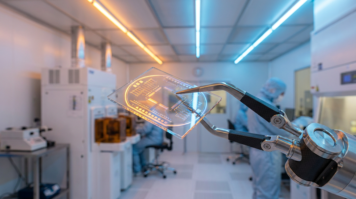
To keep Moore’s Law alive and enable the next generation of computing, the industry is turning to a material that is older than the Roman Empire: glass. Glass core substrates represent one of the most significant material shifts in semiconductor packaging in decades. By replacing flexible organic materials with rigid, ultra-flat glass, engineers can pack more transistors into a single space, transmit data faster, and prevent the warping that plagues modern chip manufacturing.[2][3]
To understand why this shift is necessary, one must look at how modern chips are built. A semiconductor package is not just a piece of silicon; it requires a substrate to translate the nanometer-scale wiring of the chip into the millimeter-scale wiring of a motherboard. As companies design massive AI processors by stitching together multiple smaller chiplets, the substrate must grow larger to accommodate them.[4][7]
The problem is thermal dynamics. Organic substrates expand and contract at a different rate than the silicon chips attached to them. Under the extreme temperatures of a data center, this mismatch causes the package to warp—sometimes bending enough to break the microscopic connections. Glass, however, possesses a coefficient of thermal expansion that closely matches silicon. This physical harmony reduces package warpage by up to 50 percent, allowing manufacturers to build massive, multi-chip packages without fear of structural failure.[2]

Beyond structural integrity, glass offers a pristine canvas for microscopic engineering. Organic resins are inherently uneven at the microscopic level, which limits how finely machines can print circuit lines. Glass is exceptionally flat and smooth. This ultra-flatness allows lithography machines to draw redistribution layers with circuit lines thinner than 2 micrometers—a density that organic cores struggle to achieve.[1][2]
The electrical properties of glass are equally transformative. In high-frequency applications, signals traveling through plastic suffer from loss, bleeding energy into the surrounding material. Glass has a dielectric constant significantly lower than silicon, meaning electrical signals can travel faster, with orders of magnitude less transmission loss. This results in cleaner, faster data transfer, which is the lifeblood of AI training workloads.[2][3]
The true magic of the technology, however, lies in Through-Glass Vias (TGVs). Because glass is uniform, manufacturers can use highly focused lasers to blast microscopic elevator shafts directly through the substrate. These TGVs allow vertical electrical connections at a density up to ten times higher than what is possible with plastic, creating ultra-fast data highways between the top and bottom of the chip package.[1][7]
The true magic of the technology, however, lies in Through-Glass Vias (TGVs).
Looking further ahead, glass offers a capability that opaque plastic never could: transparency. Researchers are already exploring ways to embed optical waveguides directly into the glass substrate. In the future, this could allow chips to transmit data using pulses of light rather than electrical currents—a concept known as co-packaged optics—drastically reducing power consumption and heat generation.[2][3]

Recognizing these immense benefits, a global race has erupted to bring glass substrates to mass production. Intel was the early pioneer, investing heavily in a billion-dollar research line in Arizona and declaring glass the key to achieving one trillion transistors in a single package by 2030. The company successfully demonstrated early samples combining its advanced packaging with glass cores, proving the concept was viable.[1][4]
However, the economics of pioneering new manufacturing techniques are daunting. Recent industry reports indicate that under its new leadership, Intel is pivoting its strategy. Rather than building the glass substrates entirely in-house, the company is reportedly looking to outsource the manufacturing to specialized vendors. This leaner approach allows the company to reduce development costs and accelerate adoption by tapping into a maturing external supply chain.[5]
Meanwhile, South Korean tech giants are aggressively moving to fill the manufacturing void. Samsung has formed a cross-departmental alliance, combining the semiconductor expertise of Samsung Electronics, the substrate knowledge of Samsung Electro-Mechanics, and the glass processing mastery of Samsung Display. This unique, vertically integrated ecosystem aims to commercialize glass interposers and substrates as early as 2026 or 2027.[6]
Other specialized players are also ramping up. SKC’s subsidiary, Absolics, has established pilot lines and is diversifying its supply chain to prepare for mass production. Japanese firms, leveraging decades of experience in display glass and precision optics, are similarly adapting their legacy technologies to serve the semiconductor market. Analysts project the global market for glass in semiconductors could reach $4.4 billion by 2036.[1][3]

Despite the momentum, the transition is not without significant hurdles. The most obvious challenge is the material's inherent brittleness. Handling ultra-thin glass panels—often less than 100 micrometers thick—in high-speed robotic assembly lines requires entirely new equipment to prevent micro-cracks and catastrophic shattering.[7]
Yield rates also remain a closely guarded industry concern. Creating millions of flawless Through-Glass Vias without compromising the structural integrity of the panel is a metallurgical and optical balancing act. A single microscopic fracture can render an entire substrate useless, making the current cost of glass packaging substantially higher than traditional methods.[6]
Because of these costs, glass will not replace organic substrates in everyday consumer laptops or smartphones anytime soon. Instead, the two technologies will coexist. Glass will debut at the absolute high end of the market—powering the massive, power-hungry AI accelerators and data center servers where its thermal and electrical advantages justify the premium.[3][7]

As the artificial intelligence era demands exponentially more computing power, the industry can no longer rely solely on shrinking transistors. The future of computing requires a stronger, faster, and cooler foundation. By turning to glass, engineers are ensuring that the physical infrastructure of the digital age can keep pace with its software ambitions.[7]
How we got here
Sep 2023
Intel publicly announces its commitment to glass substrates for advanced packaging, targeting mass production by the end of the decade.
Jan 2024
Samsung forms a cross-departmental alliance to accelerate the research and development of glass substrate chip packaging.
Jan 2026
Intel debuts its first sample combining EMIB packaging with a glass core substrate at NEPCON Japan.
Mid 2026
Multiple specialized vendors and South Korean firms ramp up pilot lines, preparing for commercial-scale deployment.
Viewpoints in depth
Advanced Packaging Innovators
Argues that glass is the mandatory next step to overcome the thermal and physical limits of AI chip scaling.
For companies pushing the absolute limits of computing power, glass is not a luxury—it is a physical necessity. Innovators in this camp argue that organic materials have reached the end of their evolutionary runway. As AI models require increasingly massive processors, the thermal expansion mismatch of plastic substrates creates unacceptable failure rates. By transitioning to glass, these companies believe they can unlock the path to one trillion transistors in a single package, ensuring that hardware can keep pace with software demands.
Supply Chain Pragmatists
Focuses on the immediate challenges of yield rates, manufacturing costs, and the necessity of outsourcing to specialized vendors.
While acknowledging the theoretical benefits of glass, pragmatists in the foundry and supply chain sectors are focused on the harsh realities of mass production. Glass is inherently brittle, and creating millions of microscopic Through-Glass Vias without introducing fatal micro-cracks is incredibly difficult. This camp emphasizes that achieving profitable yield rates will require entirely new handling equipment and specialized expertise. Consequently, they advocate for a decentralized approach, where chip designers outsource substrate manufacturing to dedicated materials companies rather than attempting to build it all in-house.
Materials Scientists
Highlights the long-term physical and optical properties of glass, envisioning a future of light-based data transmission.
Beyond solving today's thermal and electrical bottlenecks, materials scientists view glass as the bridge to the next era of computing: photonics. Because glass is transparent, it opens the door to embedding optical waveguides directly into the substrate. This camp argues that the ultimate value of glass lies not just in better electrical wiring, but in the eventual ability to transmit data using pulses of light. This co-packaged optics approach could drastically reduce the massive power consumption of modern data centers, fundamentally changing how computers are built.
What we don't know
- Exactly when the manufacturing yield rates for glass substrates will become high enough to make them cost-competitive with high-end organic substrates.
- Which specific outsourcing partners Intel will ultimately select to supply its glass core substrates.
- How quickly the technology will trickle down from enterprise AI servers to consumer-grade electronics.
Key terms
- Substrate
- The foundational layer that connects a microscopic semiconductor chip to the main circuit board.
- Organic Resin
- The traditional plastic-like material used for chip substrates, which is now reaching its thermal and physical limits.
- Through-Glass Vias (TGVs)
- Microscopic vertical holes laser-drilled into glass to allow electrical signals to pass through the substrate.
- Warpage
- The bending or deformation of a chip package caused by uneven expansion under high heat.
- Co-packaged Optics
- An emerging technology that uses light instead of electricity to transmit data directly within the chip package.
Frequently asked
Why can't we just keep using plastic substrates?
As AI chips grow larger and run hotter, traditional organic plastic substrates warp under the heat and cannot support the ultra-fine microscopic wiring needed for next-generation performance.
Will glass substrates make computers cheaper?
Initially, no. Glass substrates are complex to manufacture and will first be used in high-end AI servers and data centers where performance justifies the premium cost.
Is the glass used in chips fragile?
While glass is inherently brittle, the semiconductor industry uses specialized, highly durable formulations and advanced robotic handling techniques to prevent micro-cracks during manufacturing.
When will glass substrates be widely used?
Pilot lines are currently active, with major manufacturers targeting commercial mass production between 2026 and 2028 for high-performance computing applications.
Sources
Source coverage
7 outlets
3 viewpoints surfaced


[1]TrendForceAdvanced Packaging Innovators
Glass Substrates Ignite Global Race Toward Mass Production
Read on TrendForce →[2]SemiEngineeringMaterials Scientists
Glass Substrates Gain Traction For Advanced Packaging
Read on SemiEngineering →[3]IDTechExMaterials Scientists
Glass in Semiconductors 2026-2036: Applications, Emerging Technologies, and Market Insights
Read on IDTechEx →[4]WCCFTechSupply Chain Pragmatists
Intel-Partner, Amkor, Says Glass Substrates Will See First Commercialization Within Three Years
Read on WCCFTech →[5]TechPowerUpSupply Chain Pragmatists
Intel Reportedly Pivots on In-House Glass Substrate Manufacturing
Read on TechPowerUp →[6]Global News TopAdvanced Packaging Innovators
Samsung Group builds semiconductor, package substrate and interposer ecosystem
Read on Global News Top →[7]Factlen Editorial TeamMaterials Scientists
Synthesis by Factlen editorial team
Read on Factlen Editorial Team →

Every angle. Every day.
Get technology stories with full source coverage and perspective breakdowns delivered to your inbox.