Nanoscale Sculpting Breakthrough Pushes Superconductors Closer to Real-World Use
Researchers in Sweden have discovered that subtly sculpting the foundational layer beneath ultrathin superconductors allows them to operate at higher temperatures and withstand stronger magnetic fields. The breakthrough clears a major hurdle in the quest for zero-loss energy transmission and ultra-efficient electronics.
By Factlen Editorial Team
- Materials Scientists
- Researchers focused on the structural and chemical properties of the superconducting interface.
- Tech & Energy Industry
- Stakeholders looking to commercialize zero-loss electrical transmission to reduce global power consumption.
- Quantum Computing Researchers
- Physicists seeking robust superconducting circuits to stabilize fragile quantum states.
What's not represented
- · Environmental advocates focused on e-waste from new hardware cycles
- · Grid operators managing the transition to zero-loss infrastructure
Why this matters
Digital devices and data centers currently consume up to 12% of global electricity, much of it lost as heat due to electrical resistance. This breakthrough clears a major engineering hurdle for zero-loss superconductors, paving the way for hyper-efficient power grids, cheaper MRI machines, and vastly more powerful quantum computers.
Key points
- Researchers successfully sculpted the substrate beneath a superconductor to enhance its performance.
- The nanoscale "hills and valleys" allow the material to withstand higher temperatures and stronger magnetic fields.
- The breakthrough uses YBCO, a well-known copper-oxide superconductor, layered over magnesium oxide.
- The advance could drastically reduce the 6-12% of global electricity currently consumed by data centers.
- More resilient superconductors are also critical for cheaper MRI machines and stable quantum computers.
The holy grail of electrical engineering—transmitting power with absolutely zero energy loss—just took a significant step out of the laboratory and toward the real world. Researchers at Sweden's Chalmers University of Technology have unveiled a novel technique that allows superconducting materials to function at higher temperatures and under vastly stronger magnetic fields than previously thought possible. For decades, the fragility of the superconducting state has been the primary bottleneck preventing a revolution in global energy grids and ultra-efficient electronics. By rethinking the physical foundation upon which these materials are built, the Swedish team has bypassed a chemical roadblock that has frustrated physicists for years, offering a highly practical engineering pathway to stabilize these remarkable materials in harsh, real-world conditions.[1][2]
Superconductors are unique materials that, when cooled below a specific critical temperature, lose all electrical resistance. In a perfect superconducting loop, an electrical current could flow forever without losing a single electron to heat or friction. While they hold the potential to revolutionize everything from municipal power grids to next-generation quantum computers, their extreme environmental sensitivity has kept them largely confined to highly controlled, cryogenically cooled research environments. The moment a traditional high-temperature superconductor is exposed to the strong magnetic fields required for industrial applications, or when its temperature fluctuates even slightly, the zero-resistance state collapses, reverting the material back to a normal, inefficient conductor.[4][5]
The primary hurdle for commercialization has always been this environmental vulnerability. Engineers have spent decades trying to chemically dope and tweak these materials to make them more robust, but the atomic structures are notoriously stubborn. High-temperature superconductors, particularly the copper-oxide compounds known as cuprates, are incredibly difficult to modify chemically once they have been manufactured. Recognizing this limitation, the Chalmers University team decided to tackle the vulnerability from a completely different angle. Instead of altering the chemical makeup of the superconductor itself, they focused their attention on redesigning the physical foundation—the substrate—that the material rests upon during the fabrication process.[3][4]
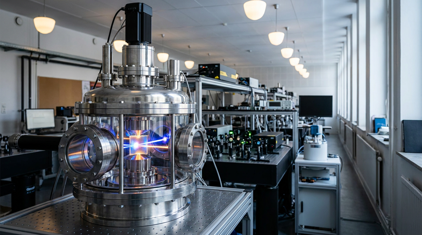
Working with a well-known cuprate superconductor called yttrium barium copper oxide (YBCO), the researchers turned their focus to the magnesium oxide (MgO) substrate used as a template for growing the ultrathin films. The superconducting layer used in these applications is astonishingly thin—often measuring just a few nanometers, which is less than one-millionth the thickness of a human hair. Because this layer is so delicate, its atomic structure is heavily influenced by the surface it is grown on. The breakthrough came when the team realized that by mechanically manipulating the MgO substrate, they could force the YBCO layer into a more advantageous structural alignment, fundamentally altering its electronic properties without changing its chemical recipe.[2][6]

To achieve this, the team utilized advanced nanoscale lithography to sculpt the magnesium oxide substrate before applying the superconductor. They carved a microscopic, highly precise pattern of hills and valleys into the foundational layer. When the ultrathin YBCO film was subsequently grown on top of this sculpted terrain, the atoms of the superconductor were forced to settle into a uniquely strained configuration, conforming to the undulating surface below. This mechanical strain created an altered electronic landscape at the exact interface between the two materials, acting as a structural anchor that locked the superconducting state into place and prevented it from degrading under external stress.[1][2]
To achieve this, the team utilized advanced nanoscale lithography to sculpt the magnesium oxide substrate before applying the superconductor.
The results of this nanoscale sculpting were immediate and striking. The researchers discovered that the strained YBCO film could maintain its superconductivity at significantly higher temperatures than films grown on standard, flat substrates. More importantly, the sculpted foundation allowed the material to withstand vastly stronger magnetic fields without reverting to a normal, resistive state. In traditional setups, the magnetic vortices that penetrate the material during operation move around and create electrical resistance, destroying the superconductivity. The nanoscale hills and valleys effectively pinned these magnetic vortices in place, preventing them from moving and thereby preserving the zero-loss electrical flow even under intense magnetic pressure.[3][6]
For the global technology sector, this newfound resilience is exactly what is needed to move superconductors from theoretical marvels to industrial components. Modern digital devices, hyperscale data centers, and global information and communications technology (ICT) networks currently consume an estimated 6 to 12 percent of the world's electricity. As the demand for artificial intelligence and cloud computing continues to skyrocket, this energy burden is rapidly climbing, placing unprecedented strain on aging power grids and accelerating carbon emissions. Finding a way to make computing hardware fundamentally more efficient is no longer just an economic priority; it is a critical climate imperative.[1][5]

If data centers could utilize superconducting interconnects and processors, the resulting energy savings would be monumental. Current silicon-based systems lose vast amounts of energy as heat due to inherent electrical resistance. This thermal waste not only drains power directly but also requires massive, energy-intensive cooling infrastructure to prevent the servers from melting down. Integrating zero-resistance superconducting materials would eliminate this thermal waste entirely, allowing data centers to operate at a fraction of their current power footprint while simultaneously processing information at significantly higher speeds.[3][5]
Beyond enterprise computing and energy grids, the Chalmers breakthrough has profound implications for advanced medical imaging and quantum technology. Magnetic resonance imaging (MRI) machines rely on massive superconducting magnets to generate the high-resolution scans used in hospitals worldwide. Currently, these magnets require expensive, complex liquid helium cooling systems to maintain their delicate superconducting state. By utilizing cuprate films stabilized by sculpted substrates, future MRI machines could operate with much simpler and cheaper cooling mechanisms, drastically lowering the cost of the equipment and making life-saving diagnostic technology more accessible globally.[4][5]
In the rapidly advancing realm of quantum computing, the stability of qubits is the single greatest engineering challenge. Qubits are notoriously sensitive to magnetic, thermal, and electrical interference, which causes them to lose their quantum state in a process known as decoherence. Superconducting circuits are one of the leading architectures for building quantum computers, but their fragility limits the size and reliability of the processors. Superconducting circuits built on these newly stabilized, high-tolerance cuprate films could lead to far more robust quantum processors that are less prone to error, accelerating the timeline for commercially viable quantum technology.[3][6]

While the Chalmers discovery does not immediately yield a room-temperature superconductor—the ultimate, long-sought prize of condensed matter physics—it provides a highly practical, immediate engineering pathway. By proving that mechanical manipulation of the substrate can dramatically enhance performance, the researchers have opened an entirely new frontier in materials science. It demonstrates that the physical geometry of the foundational layer is just as important as the chemical composition of the superconductor itself, offering engineers a powerful new variable to play with in the quest for perfect electrical transmission.[2][4]
The next phase of research will focus on scaling this nanoscale sculpting process from small laboratory samples to larger wafers suitable for industrial manufacturing. The team also plans to test the substrate manipulation technique on other families of superconducting materials to see if the pinning effect is universally applicable. If the method can be cost-effectively scaled and applied broadly, the transition to a zero-loss electrical infrastructure—powering everything from lossless municipal grids to hyper-efficient AI data centers—may arrive much sooner than anyone in the industry anticipated.[1][5]
How we got here
1986
High-temperature superconductivity is first discovered in cuprate materials, winning a Nobel Prize.
Early 2000s
Researchers begin growing ultrathin superconducting films on substrates to integrate them into electronics.
June 17, 2026
Chalmers University publishes findings showing that nanoscale substrate sculpting dramatically boosts superconductor resilience.
Viewpoints in depth
Materials Scientists
Researchers focused on the structural and chemical properties of the superconducting interface.
For materials scientists, the breakthrough represents a paradigm shift in how superconductors are engineered. Rather than relying solely on complex chemical doping to alter the properties of cuprates, this approach proves that mechanical manipulation of the substrate can yield profound electronic changes. They view the nanoscale sculpting technique as a versatile new tool that could theoretically be applied to various thin-film materials beyond just copper-oxide compounds, opening up new avenues for stabilizing delicate atomic structures.
Tech & Energy Industry
Stakeholders looking to commercialize zero-loss electrical transmission to reduce global power consumption.
The technology and energy sectors are primarily focused on the commercial viability of the discovery. Industry analysts emphasize that even incremental increases in magnetic field tolerance and temperature stability can translate to billions of dollars in energy savings. With artificial intelligence driving an unprecedented boom in data center construction, the industry views zero-loss superconducting interconnects as one of the few viable long-term solutions to the looming global energy crunch.
Quantum Computing Researchers
Physicists seeking robust superconducting circuits to stabilize fragile quantum states.
Quantum physicists see this development as a potential missing link for scaling quantum processors. Because qubits are highly susceptible to environmental noise and magnetic interference, building stable quantum computers has proven exceptionally difficult. Researchers argue that the ability to maintain superconductivity under stronger magnetic fields could lead to the creation of highly robust, error-resistant qubits, significantly accelerating the timeline for commercially useful quantum technology.
What we don't know
- Whether this specific nanoscale sculpting technique can be cost-effectively scaled for mass industrial manufacturing.
- If the same substrate manipulation will yield similar benefits for other classes of superconducting materials beyond cuprates.
- Exactly how much higher the critical temperature can be pushed using this mechanical strain method.
Key terms
- Superconductor
- A material that can conduct electricity with zero resistance and zero energy loss when cooled below a certain temperature.
- Cuprate
- A class of copper-oxide materials known for exhibiting superconductivity at relatively high temperatures compared to traditional metals.
- Substrate
- The foundational base layer upon which ultrathin films of other materials are grown during manufacturing.
- Nanoscale
- A scale of measurement involving dimensions of a few nanometers, where one nanometer is one-billionth of a meter.
- Qubit
- The basic unit of quantum information, which relies on delicate quantum states that can be stabilized by superconducting circuits.
Frequently asked
Does this mean we have room-temperature superconductors?
No. The materials still need to be cooled, but they can maintain their zero-resistance state at higher temperatures and under harsher conditions than before.
Why is the magnetic field tolerance important?
Many practical applications, like MRI machines and power generators, generate strong magnetic fields that normally destroy the superconducting state. This breakthrough prevents that.
How does the sculpted substrate help?
The microscopic hills and valleys force the atoms in the superconducting layer into a strained configuration, which anchors the electronic properties and prevents the material from losing its zero-resistance state.
Sources
Source coverage
6 outlets
3 viewpoints surfaced


[1]ScienceDailyQuantum Computing Researchers
New Path to Stronger Superconductors
Read on ScienceDaily →[2]Chalmers University of TechnologyMaterials Scientists
A clever nanoscale redesign solves superconductivity hurdle
Read on Chalmers University of Technology →[3]IEEE SpectrumTech & Energy Industry
Nanoscale Substrate Sculpting Pushes Cuprate Superconductors Further
Read on IEEE Spectrum →[4]Physics WorldMaterials Scientists
Sculpted substrates boost high-temperature superconductivity in cuprates
Read on Physics World →[5]WiredTech & Energy Industry
A Nanoscale Tweak Could Finally Bring Superconductors Out of the Lab
Read on Wired →[6]Nature MaterialsMaterials Scientists
Enhanced superconductivity in YBCO films via nanoscale substrate modification
Read on Nature Materials →


Every angle. Every day.
Get meta stories with full source coverage and perspective breakdowns delivered to your inbox.