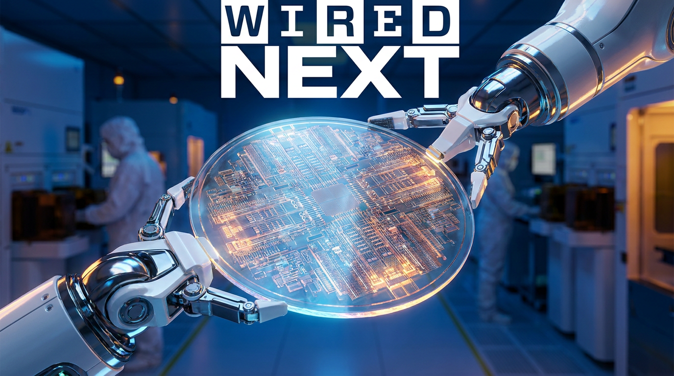
How Glass Substrates Are Solving the AI Chip Energy Crisis
As artificial intelligence pushes traditional silicon packaging to its thermal limits, the semiconductor industry is turning to glass substrates to drastically reduce power consumption and increase data speeds.
By Factlen Editorial Team
- Materials Scientists
- Focuses on the physical properties, thermal stability, and microscopic advantages of glass over organic compounds.
- Foundry Operators
- Emphasizes the practical manufacturing hurdles, equipment redesign costs, and yield rate challenges of handling fragile glass.
- Data Center Architects
- Prioritizes the massive energy savings, cooling reductions, and performance gains that glass substrates will unlock at scale.
- Technology Analysts
- Views the transition as a necessary evolutionary step to keep Moore's Law alive through advanced packaging.
What's not represented
- · Consumer electronics manufacturers
- · Environmental impact analysts
Why this matters
As AI models grow exponentially, the energy required to run them is becoming unsustainable. Glass substrates offer a physical solution to this bottleneck, promising faster, cooler, and more energy-efficient devices that will power the next decade of computing without overwhelming global power grids.
Key points
- The AI boom is pushing traditional organic chip substrates to their thermal and physical limits.
- Glass substrates offer exceptional dimensional stability, preventing the warping that destroys high-powered chips.
- The ultra-flat surface of glass allows for up to 10 times greater interconnect density.
- Shorter electrical pathways on glass significantly reduce energy loss, a crucial benefit for power-hungry data centers.
- Semiconductor foundries must redesign their manufacturing lines to handle the fragility of ultra-thin glass panels.
The artificial intelligence revolution is colliding with a physical wall. As large language models grow exponentially in size and capability, the silicon chips required to train and run them are drawing unprecedented amounts of power and generating massive heat.[3][6]
For decades, the semiconductor industry has relied on organic materials to serve as the foundational substrates that connect microscopic silicon chips to larger computer motherboards. But these traditional organic substrates are reaching their thermal and physical limits under the strain of modern computing demands.[1][4]
To keep the pace of computational progress alive, materials scientists and chip manufacturers are turning to an elegant, highly engineered solution: glass. Glass substrates are emerging as the critical breakthrough needed to build the next generation of ultra-powerful, energy-efficient microprocessors.[6]
To understand why glass is revolutionary, one must first understand the role of a substrate. A substrate is the structural backbone of a computer chip. It acts as a translator, taking the incredibly dense, microscopic wiring of a silicon die and fanning it out to the larger, macroscopic pins that plug into a computer's main circuit board.[1]

Organic substrates have performed this translation admirably for years, but they suffer from a fatal flaw under extreme stress: they warp. When subjected to the intense heat generated by modern AI accelerators, organic materials can bend and distort, breaking the fragile microscopic connections and ruining the chip.[2][4]
Glass, by contrast, possesses exceptional dimensional stability. It does not warp under high temperatures, and it remains perfectly flat at a microscopic level. This ultra-flat surface allows manufacturers to print wiring that is vastly smaller and more tightly packed than what is possible on organic materials.[2][5]
Glass, by contrast, possesses exceptional dimensional stability.
The key to this density lies in a technology called Through-Glass Vias, or TGVs. These are microscopic holes drilled directly through the glass using advanced lasers, allowing electrical signals to pass vertically through the substrate. Because glass is so stable, these vias can be placed much closer together.[1][5]
The result is a staggering increase in interconnect density. Engineers can pack up to ten times more connections into the same physical space. This means more data can flow between different parts of the chip simultaneously, drastically increasing the speed at which AI models can process information.[2][3]

Beyond speed, the shift to glass offers a massive leap in energy efficiency. In traditional packaging, electrical signals must travel relatively long distances across the substrate, losing energy as heat along the way. The ultra-dense wiring enabled by glass shortens these distances, significantly reducing power loss.[5]
For massive data centers, this efficiency is transformative. Modern AI chips can draw upwards of 400 watts of power individually, placing immense strain on global power grids and requiring expensive, energy-intensive cooling systems. Glass substrates offer a physical mechanism to curb this runaway power consumption.[3][6]
However, transitioning an entire global industry from plastic to glass is not without profound challenges. The most obvious hurdle is fragility. Semiconductor manufacturing involves moving large panels of substrate material through hundreds of robotic processing steps at high speeds.[4]
Standard cleanroom equipment is designed to handle flexible organic panels or rigid silicon wafers, not ultra-thin sheets of glass that can shatter if mishandled. Foundries are currently investing billions of dollars to redesign their manufacturing lines, developing new robotic handlers and shock-absorbing transport systems.[1][4]

Despite these manufacturing hurdles, the economic and computational incentives are too large to ignore. Major players across the semiconductor supply chain are aggressively accelerating their research and development timelines, moving glass from a laboratory curiosity to a commercial necessity.[1][6]
As the industry pushes toward commercial production later this decade, glass substrates stand as a testament to human ingenuity. By reimagining the very foundation upon which our digital world is built, engineers are ensuring that the march of technological progress can continue unimpeded.[6]
How we got here
1990s-2020s
Organic materials dominate the semiconductor substrate market, providing flexible and cost-effective packaging.
2023
Major foundries publicly announce massive R&D investments into glass substrate technology to solve AI thermal limits.
2025
The first fully functional, high-performance prototype chips packaged on glass substrates are demonstrated in labs.
2026-2030
Projected timeline for the commercial rollout of glass-packaged chips in enterprise data centers.
Viewpoints in depth
Materials Scientists
Focuses on the physical properties and thermal stability of glass.
Researchers in materials science view the shift to glass as an inevitable triumph of physics over legacy engineering. They point to peer-reviewed data showing that glass maintains its dimensional integrity at temperatures that cause organic polymers to fail catastrophically. By eliminating substrate warpage, scientists argue that glass provides the perfect, ultra-flat canvas required to push photolithography to its absolute limits, enabling microscopic wiring that was previously impossible.
Foundry Operators
Emphasizes the practical manufacturing hurdles and equipment costs.
For the engineers tasked with actually building these chips, glass represents a terrifying logistical challenge. Foundry operators emphasize that standard cleanroom robotics are calibrated for the flexibility of organics or the specific rigidity of silicon. Introducing ultra-thin, highly brittle glass panels requires a ground-up redesign of transport mechanisms, chemical etching processes, and handling protocols. Their primary concern is maintaining high yield rates; a single shattered glass panel can contaminate a cleanroom and halt a multi-million dollar production line.
Data Center Architects
Prioritizes the massive energy savings and performance gains at scale.
Those responsible for building and maintaining the massive infrastructure behind AI models see glass substrates as a financial and ecological lifeline. Data center architects are currently battling a crisis of power density, where the electricity required to run and cool modern AI racks is outpacing grid capacity. They argue that the energy efficiency gained by shortening interconnect distances on glass substrates is not just a performance boost, but a necessary intervention to keep the operational costs of AI from spiraling out of control.
What we don't know
- Exactly how high the manufacturing yield rates will be during the initial commercial rollout of glass substrates.
- Whether the cost of retooling foundries for glass will temporarily increase the price of high-end AI accelerators.
- How long it will take for glass substrate technology to trickle down from enterprise data centers to everyday consumer electronics.
Key terms
- Substrate
- The structural base layer that physically supports a microchip and provides the electrical connections to the rest of the computer.
- Advanced Packaging
- The process of combining multiple complex silicon chips into a single, highly efficient package to boost performance.
- Interconnects
- The microscopic wires and pathways that allow electrical signals to travel between different parts of a computer chip.
- Through-Glass Via (TGV)
- Microscopic holes drilled through a glass substrate using lasers, allowing electrical signals to pass vertically through the material.
Frequently asked
What exactly is a semiconductor substrate?
A substrate is the foundational layer that connects the microscopic wiring of a silicon chip to the larger, macroscopic pins on a computer's motherboard.
Why are traditional substrates failing?
Traditional substrates are made of organic, plastic-like materials that can warp and distort under the extreme heat generated by modern, high-powered AI chips.
When will glass substrates be in consumer devices?
Major semiconductor foundries are targeting commercial production for high-performance computing between 2026 and 2030, with consumer devices likely following shortly after.
Sources
Source coverage
6 outlets
4 viewpoints surfaced


[1]IEEE SpectrumFoundry Operators
Why the Semiconductor Industry is Shifting to Glass Substrates
Read on IEEE Spectrum →[2]Nature ElectronicsMaterials Scientists
Thermal and electrical properties of glass-core substrates for advanced packaging
Read on Nature Electronics →[3]MIT Technology ReviewData Center Architects
The materials science breakthrough saving AI from melting down
Read on MIT Technology Review →[4]Semiconductor EngineeringFoundry Operators
Glass Substrates Gaining Traction in Advanced Packaging
Read on Semiconductor Engineering →[5]Applied Physics LettersMaterials Scientists
High-density interconnects on glass for next-generation microelectronics
Read on Applied Physics Letters →[6]Factlen Editorial TeamTechnology Analysts
Synthesis by Factlen editorial team
Read on Factlen Editorial Team →


Every angle. Every day.
Get technology stories with full source coverage and perspective breakdowns delivered to your inbox.