TSMC Begins Volume Production of 2nm GAAFET Chips, Confirming Next-Gen Node Leadership
Taiwan Semiconductor Manufacturing Company has officially ramped up high-volume manufacturing of its 2-nanometer chips, marking the industry's historic transition to Gate-All-Around transistor architecture.
By Factlen Editorial Team
- Leading-Edge Foundries
- Focused on stabilizing yields, managing extreme manufacturing costs, and winning the architectural race.
- Fabless Innovators
- Willing to pay massive premiums for early access to node shrinks to maintain product leadership.
- Supply Chain Analysts
- Focused on capacity growth, geographic concentration, and the economic realities of the Angstrom era.
What's not represented
- · Environmental groups monitoring the massive energy and water demands of 2nm fabs
- · Mid-tier tech companies priced out of the bleeding edge
Why this matters
The transition to 2nm silicon breaks through the 'thermal wall' that threatened to stall technological progress. By drastically reducing power consumption and heat, these chips will enable the next massive leap in artificial intelligence capabilities and significantly extend the battery life of consumer devices.
Key points
- TSMC has entered high-volume manufacturing for its 2nm (N2) process.
- The 2nm node marks the industry's shift from FinFET to GAAFET architecture.
- N2 chips offer up to 30% power reduction or 15% performance gains over 3nm.
- TSMC expects 2nm capacity to grow at a 70% compound annual rate through 2028.
- Apple, AMD, and Nvidia have already secured the majority of early production capacity.
- Wafer costs have surged to an estimated $30,000 due to manufacturing complexity.
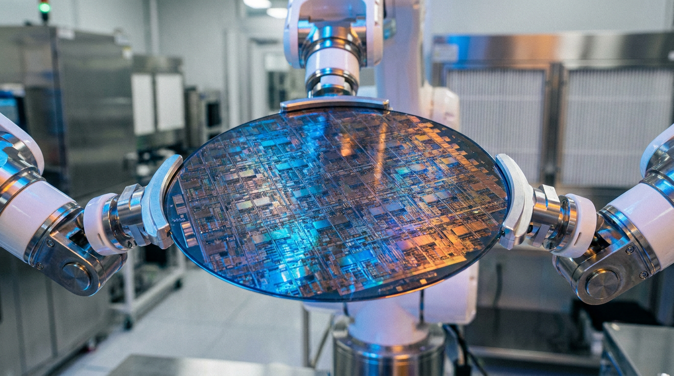
The semiconductor industry has officially crossed into the Angstrom era. Taiwan Semiconductor Manufacturing Company (TSMC) has commenced high-volume manufacturing of its 2-nanometer (N2) process, marking the most significant architectural shift in chip design in over a decade.[1][5]
The transition to the 2nm node represents the retirement of the FinFET (Fin Field-Effect Transistor) architecture, which has served as the foundational building block of the global technology economy since the 22nm generation. In its place, TSMC has successfully commercialized Gate-All-Around (GAAFET) nanosheet transistors.[1][5]
This architectural pivot is not merely an incremental upgrade; it is a fundamental survival tactic for an industry rapidly approaching a physical thermal wall. As artificial intelligence models scale exponentially, data center power envelopes routinely exceed 1,000 watts per rack unit, demanding silicon that can compute more without melting down.[5]
The technical necessity for GAAFET stems from the physical limitations of shrinking silicon. In a FinFET structure, the gate wraps around three sides of a vertical fin channel. As transistors shrank toward the 2nm scale, these fins became so thin that the gate began to lose electrostatic control over the bottom of the channel, resulting in catastrophic power leakage even when the transistor was switched off.[5]

GAAFET solves this by fundamentally reshaping the channel. Instead of a vertical fin, the channel consists of multiple horizontally stacked silicon nanosheets. The gate material completely surrounds these nanosheets on all four sides, providing 360-degree electrostatic control and virtually eliminating unwanted current leakage.[1][5]
The practical results of this 360-degree control are striking. TSMC's N2 node delivers a 10% to 15% performance improvement at the same power level compared to its previous 3nm (N3E) generation. Alternatively, chip designers can opt for a 25% to 30% reduction in power consumption while maintaining the exact same performance.[1][4]

Beyond the transistor architecture itself, TSMC has introduced super-high-performance metal-insulator-metal (SHPMIM) capacitors to the N2 power delivery network. These capacitors offer more than twice the capacitance density of previous designs while cutting resistance in half, dramatically improving power stability for high-frequency AI accelerators.[1][4]
Beyond the transistor architecture itself, TSMC has introduced super-high-performance metal-insulator-metal (SHPMIM) capacitors to the N2 power delivery network.
The physical rollout of this technology is currently centered entirely in Taiwan. Volume production is ramping up simultaneously at Fab 20 in Baoshan, near the company's Hsinchu headquarters, and at Fab 22 in Kaohsiung.[1][3]
The scale of TSMC's ambition for the N2 node is unprecedented. At the company's recent technology symposium, executives projected that 2nm chip capacity will grow at a compound annual rate of 70% from 2026 through 2028.[3][6]
By the end of 2026, TSMC expects its total 2nm capacity to reach 100,000 wafers per month. Output in this first full year of production is already projected to be 45% higher than the equivalent first-year output of the 3nm node back in 2023.[4][6]

However, the bleeding edge of physics comes at a steep financial premium. Industry analysts estimate that a single 2nm wafer costs approximately $30,000—a 50% price hike compared to the N3 generation. This surge is driven by the extreme complexity of manufacturing nanosheets and the intensive use of extreme ultraviolet lithography.[4][5]
Despite the eye-watering costs, TSMC's order books are fully booked. Apple has reportedly secured more than half of the initial 2026 capacity for its upcoming silicon, while other major fabless designers—including AMD, MediaTek, Nvidia, and Qualcomm—have locked in their own allocations.[2][4]
The successful ramp of N2 also solidifies TSMC's position against its primary foundry rivals. While Samsung aggressively pursued GAAFET technology earlier with its 3nm node, and Intel is pushing its 18A process, TSMC's ability to achieve stable yields of 70% to 80% on a brand-new architecture has kept the majority of high-volume customers firmly in its camp.[2][5]
Looking ahead, the base N2 node is only the foundation. Starting in late 2026, TSMC plans to introduce N2P, a performance-enhanced variant. Shortly thereafter, the company will roll out the A16 node, which will introduce Super Power Rail backside power delivery—a technique that moves power routing to the back of the wafer to free up space for logic routing.[1][4]

Geopolitically, the N2 rollout underscores Taiwan's enduring gravity in the global supply chain. While TSMC is expanding its footprint with fabs in Arizona, Japan, and Germany, the company's most advanced nodes and the critical yield learning phase remain strictly anchored in its domestic facilities.[2][6]
As 2026 progresses, the focus will shift from foundry yields to consumer benchmarks. The first wave of 2nm-powered smartphones and AI servers will soon hit the market, translating years of atomic-level engineering into tangible leaps in battery life and computational intelligence.[5]
How we got here
2022
TSMC begins high-volume production of its 3nm (N3) FinFET node.
July 2024
TSMC initiates risk production for the 2nm (N2) process.
Late 2025
High-volume manufacturing of N2 quietly commences in Taiwan.
Early 2026
Yields stabilize between 70% and 80%, prompting a massive capacity expansion.
Late 2026
TSMC targets 100,000 N2 wafers per month and prepares to launch the N2P variant.
Viewpoints in depth
Leading-Edge Foundries
TSMC, Samsung, and Intel view the 2nm transition as the ultimate test of their manufacturing prowess.
For TSMC, stabilizing GAAFET yields proves their execution remains unmatched, allowing them to maintain dominance in the foundry market. Meanwhile, rivals like Samsung and Intel see the architectural reset from FinFET to GAAFET as their best window to capture market share, aggressively pushing their own equivalent nodes to court fabless designers.
Fabless Chip Designers
Companies like Apple, AMD, and Nvidia view the $30,000-per-wafer cost as a necessary premium.
In the highly competitive AI and premium mobile markets, the power-efficiency gains of 2nm are critical. Designers argue that paying a 50% premium over 3nm is the only way to unlock advanced on-device AI capabilities and prevent massive data centers from hitting thermal limits. For these companies, performance leadership justifies the extreme manufacturing costs.
Geopolitical Analysts
Supply chain experts note that keeping the N2 ramp strictly in Taiwan reinforces TSMC's 'silicon shield.'
While TSMC is building international fabs in the US, Japan, and Europe, analysts point out that the absolute bleeding edge—including the critical yield learning phase—remains geographically concentrated in Baoshan and Kaohsiung. This strategy ensures that Taiwan remains indispensable to the global technology ecosystem, maintaining its strategic leverage.
What we don't know
- How quickly TSMC can scale extreme ultraviolet (EUV) lithography equipment to meet the 100,000 wafer-per-month target.
- Whether the $30,000 wafer cost will force consumer electronics prices significantly higher in late 2026.
Key terms
- GAAFET (Gate-All-Around)
- A transistor architecture where the gate completely surrounds the channel, offering superior electrical control compared to older designs.
- FinFET
- The previous generation of transistor design where the gate wrapped around three sides of a vertical silicon 'fin'.
- Node
- A specific generation of semiconductor manufacturing technology, historically named after a physical measurement but now used as a generational label.
- Wafer
- A thin slice of semiconductor material, usually silicon, upon which microcircuits are fabricated.
- Yield
- The percentage of functional, defect-free chips produced on a single silicon wafer.
- Backside Power Delivery
- An upcoming technique that routes power to transistors from the back of the silicon wafer, freeing up space for data routing on the front.
Frequently asked
What does '2nm' actually mean?
It is a marketing term for a generation of chips. It does not mean the physical transistors are exactly 2 nanometers wide, but rather denotes a specific leap in density and efficiency over the previous 3nm generation.
What is GAAFET?
Gate-All-Around Field-Effect Transistor. It is a new architecture where the gate material completely surrounds the silicon channel on all four sides, preventing power leakage.
Why are 2nm chips so expensive?
The manufacturing process requires extreme ultraviolet (EUV) lithography and highly complex atomic-level engineering to stack silicon nanosheets, driving wafer costs to an estimated $30,000.
When will consumers see 2nm devices?
The first consumer devices featuring 2nm silicon, primarily flagship smartphones and high-end AI accelerators, are expected to hit the market in late 2026.
Sources
Source coverage
6 outlets
3 viewpoints surfaced


[1]Tom's HardwareLeading-Edge Foundries
TSMC quietly begins volume production of 2nm-class chips
Read on Tom's Hardware →[2]EE TimesLeading-Edge Foundries
TSMC 2-nm Node to Lead Rivals for Years
Read on EE Times →[3]Focus TaiwanSupply Chain Analysts
TSMC sees 70% annual growth in 2nm capacity through 2028
Read on Focus Taiwan →[4]SemiWikiFabless Innovators
TSMC 2nm Capacity and Pricing Dynamics
Read on SemiWiki →[5]Wedbush SecuritiesFabless Innovators
The 2nm Arms Race: Winners and Losers in the AI Era
Read on Wedbush Securities →[6]Taipei TimesSupply Chain Analysts
TSMC expects 70% 2nm growth
Read on Taipei Times →
Every angle. Every day.
Get technology stories with full source coverage and perspective breakdowns delivered to your inbox.