How Glass Substrates Are Solving the AI Chip Packaging Bottleneck
As artificial intelligence chips grow too large and hot for traditional plastic foundations, the semiconductor industry is turning to ultra-flat glass to unlock the next generation of computing power.
By Factlen Editorial Team
- Integrated Foundries
- View glass substrates as a critical in-house capability to maintain dominance in advanced packaging.
- Substrate Pioneers
- Believe dedicated material science and first-mover manufacturing will capture the market.
- Industry Analysts
- View the transition as inevitable but caution about near-term manufacturing hurdles and high costs.
What's not represented
- · Environmental Advocates (assessing the energy and recycling impact of mass glass substrate manufacturing)
- · Fabless Chip Designers (Nvidia, AMD, Apple - the ultimate end-users of the technology)
Why this matters
The physical limits of plastic chip packaging have become the primary bottleneck for advancing artificial intelligence. By transitioning to glass, the industry can pack exponentially more computing power into data centers, enabling breakthroughs from advanced AI models to 6G networks.
Key points
- Traditional plastic chip substrates are warping under the immense heat and size of modern AI processors.
- Glass substrates offer superior thermal stability and ultra-flat surfaces, preventing warpage during manufacturing.
- The transition to glass enables a 10x increase in interconnect density and a 50% reduction in package thickness.
- Major players like Intel, TSMC, Samsung, and Absolics are racing to commercialize the technology before 2030.
The artificial intelligence boom is currently colliding with a stubborn physical wall. As technology giants race to build increasingly powerful AI models, the silicon chips required to process those massive datasets are growing exponentially larger. However, the primary bottleneck threatening to slow this progress is not the silicon itself, but rather the foundational material that the chips sit on. For decades, the semiconductor industry has relied on organic resins—specifically a specialized plastic known as Ajinomoto Build-up Film (ABF)—to form the core of chip packages. This substrate acts as the critical bridge, routing microscopic electrical signals from the delicate silicon die down to the main circuit board. While plastic has served the industry well for years, the sheer size and thermal output of modern AI accelerators are pushing these organic materials past their breaking point.[1][7]
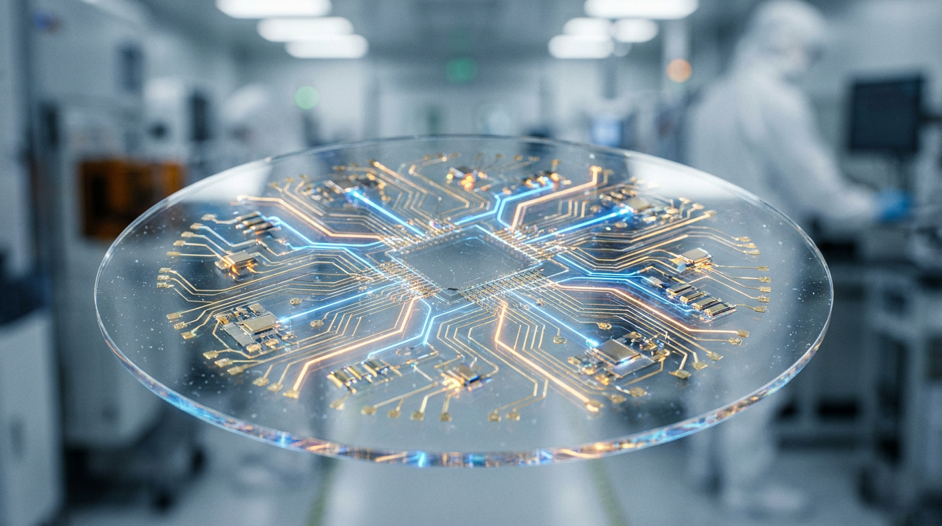
As AI processors expand to the size of a drink coaster, these plastic substrates are buckling under the pressure. During the intense heat of the manufacturing and reflow processes, large organic substrates tend to warp, bending much like a potato chip left in the sun. This warpage is catastrophic at the microscopic level; it breaks delicate electrical connections, ruins expensive silicon components, and ultimately caps how large a chip can physically be built. The industry's solution to this impending crisis is a radical shift in material science: replacing the plastic core with glass. Glass substrates are rapidly emerging as the definitive next-generation packaging technology, promising to solve the thermal and mechanical limits of organic materials and unlock the next era of high-performance computing.[1][5]
"After a decade of research, Intel has achieved industry-leading glass substrates for advanced packaging," stated Babak Sabi, Intel's senior vice president of Assembly and Test Development, when the company unveiled its roadmap. Intel and other industry leaders view glass as absolutely essential to keeping Moore's Law alive into the 2030s. The mechanical properties of glass make it an ideal candidate for massive AI chips. Unlike plastic, glass is exceptionally flat and dimensionally stable, meaning it does not warp or degrade under high temperatures. This rigid stability allows manufacturers to pack silicon components much closer together without fear of structural failure, fundamentally changing the design rules for chip architects.[2][7]

The transition to this new material relies on a manufacturing breakthrough known as Through-Glass Vias (TGVs). Instead of routing signals through layers of flexible plastic, high-precision lasers are used to drill microscopic holes directly through the solid glass core. Because glass is so exceptionally smooth and rigid, these holes can be placed incredibly close together with near-perfect accuracy. The resulting performance gains are staggering. Glass substrates can increase the interconnect density between chips by a factor of ten, allowing vastly more data to flow between components.[1][3]
Beyond just data density, the physical footprint of the chips is dramatically improved. Glass substrates allow for up to a 50% reduction in overall package thickness. In the cramped, power-hungry environment of a modern data center, every millimeter matters. Thinner packages free up critical vertical space, allowing engineers to implement enhanced power delivery networks and more robust liquid cooling systems directly on top of the silicon. This thermal management is vital, as next-generation AI chips are expected to draw unprecedented amounts of electricity, generating heat that would easily warp or melt older packaging technologies. By moving to glass, data center operators can pack more computing power into the same physical racks while simultaneously reducing the energy required to keep the systems cool.[3][7]
Beyond just data density, the physical footprint of the chips is dramatically improved.
This unprecedented density and thermal stability are crucial for the modern "chiplet" era of semiconductor design. Rather than attempting to manufacture one giant, flawless piece of silicon—which is incredibly difficult and expensive—companies now stitch together multiple smaller, specialized chips, known as chiplets, into a single unified package. Glass provides the perfect, ultra-flat canvas required to integrate logic processors, high-bandwidth memory, and power delivery chiplets seamlessly. Because the surface is perfectly smooth, the microscopic bridges connecting these chiplets can be printed with extreme precision, ensuring that the modular components communicate just as fast as if they were carved from a single piece of silicon. This heterogeneous integration is the only viable path forward for scaling AI performance.[2][4][7]

"Glass core substrates enable manufacturers to push the boundaries of semiconductor performance," notes Sean Chiu, Asia Business Development Manager at specialty glass maker SCHOTT. Beyond raw computational speed, the material's low signal loss and high energy efficiency are expected to unlock entirely new applications across multiple industries. In the telecommunications sector, glass substrates are being heavily researched for upcoming 6G networks, where ultra-high-frequency signals suffer from severe degradation when passing through traditional plastics. Similarly, the ability to shrink high-performance processors without sacrificing battery life could finally deliver lightweight augmented reality hardware that feels indistinguishable from ordinary eyeglasses, moving the technology out of the realm of bulky headsets.[6][7]
Recognizing the massive stakes involved, a fierce global race has ignited to commercialize the technology. While Intel has been developing glass substrates internally for over a decade, South Korean and Taiwanese firms are aggressively accelerating their own timelines to prevent the American giant from dictating future industry standards. If Intel succeeds in establishing the baseline design rules for glass packaging, fabless chip companies worldwide could be compelled to follow its specifications, potentially posing a significant threat to the broader Asian semiconductor ecosystem. This geopolitical and corporate rivalry has transformed glass substrates from a niche material science project into a top strategic priority for national technology sectors.[5][7]
SKC subsidiary Absolics has taken an early and aggressive lead in dedicated manufacturing, constructing the world's first mass-production facility for glass substrates in Covington, Georgia. Backed by significant funding from the U.S. CHIPS Act, Absolics aims to transition from prototype sampling to full-scale commercial production ahead of traditional foundries. By building a dedicated facility on American soil, the company is positioning itself as an indispensable supplier in the new AI supply chain. They are betting that the specialized expertise required to drill and metallize glass will allow them to offer their advanced panels to any chip designer or foundry that needs them, effectively democratizing access to the technology rather than keeping it locked within a single corporate walled garden.[3][7]

Meanwhile, the world's largest integrated chipmakers are refusing to be left behind. Samsung has launched a comprehensive strategy, combining the expertise of its memory and foundry divisions to develop a complete, end-to-end glass ecosystem. By optimizing both the silicon and the glass substrate in tandem, Samsung hopes to offer clients a turnkey solution for next-generation AI accelerators. Not to be outdone, TSMC—the world's dominant contract chipmaker—recently disclosed successful validation tests for applying glass substrates to its advanced CoWoS (Chip-on-Wafer-on-Substrate) packaging. This signals TSMC's clear intent to dominate this new frontier just as it has dominated traditional silicon manufacturing, ensuring that its largest customers, like Nvidia and AMD, do not have to look elsewhere for their packaging needs.[5][7]
The financial implications of this technological arms race are massive. Market intelligence firm IDTechEx projects that the global market for glass in semiconductors will reach $4.40 billion by 2036, growing at a rapid compound annual rate of 14.2%. This growth is not just driven by the substrates themselves, but by the entirely new ecosystem of manufacturing equipment, optical inspection tools, and specialized chemical treatments required to process the glass panels. Because the existing machinery used for plastic substrates cannot simply be repurposed for glass, an entire secondary market of equipment vendors is springing up to support the transition. Companies that can successfully navigate and supply this shift stand to capture a significant share of the most lucrative segment of the semiconductor market.[4][7]

Despite the widespread optimism and massive capital investments, the transition from plastic to glass remains fraught with significant engineering hurdles. Glass is inherently brittle, and preventing microscopic cracks during the high-speed drilling, metallization, and handling processes remains a formidable challenge. A single micro-crack can compromise an entire panel, destroying thousands of dollars worth of materials. Furthermore, the manufacturing costs are currently prohibitive for anything other than the most expensive, high-margin AI accelerators. Widespread adoption across consumer electronics is still years away. Yet, the consensus across the semiconductor landscape is clear: the physical limits of plastic have been reached. As artificial intelligence continues to demand exponentially more computing power, the foundation of the future will undoubtedly be built on glass.[1][3][7]
How we got here
2018
SKC begins earnest development of glass substrates for semiconductor packaging.
2021
Absolics is established to commercialize glass substrates, later building a facility in Georgia.
Sep 2023
Intel publicly announces its commitment to glass substrates, targeting mass production by 2030.
Jan 2026
Intel debuts its first sample combining EMIB packaging with a glass core substrate at NEPCON Japan.
Jun 2026
TSMC discloses successful validation results for applying glass substrates to its advanced CoWoS packaging.
Viewpoints in depth
Integrated Foundries
Giants like Intel, TSMC, and Samsung view glass substrates as a critical in-house capability to maintain dominance in advanced packaging.
For the world's largest chipmakers, controlling the packaging substrate is just as important as etching the silicon itself. Intel has invested a decade of research into glass to ensure it sets the design standards for the 2030s. Meanwhile, TSMC and Samsung are aggressively validating their own glass-core technologies, fearing that relying on third-party substrate suppliers could cost them their leadership in the highly lucrative AI accelerator market.
Specialized Substrate Pioneers
Dedicated material science firms believe their singular focus and early manufacturing investments will capture the market.
Companies like SKC's Absolics and specialty glass makers argue that handling and metallizing glass requires entirely different expertise than traditional silicon manufacturing. By building dedicated facilities—such as Absolics' plant in Georgia—these pioneers aim to establish themselves as the indispensable middle layer of the supply chain, providing the foundational glass panels that fabless chip designers and foundries will ultimately rely on.
Industry Analysts
Market researchers view the transition as inevitable but caution about near-term manufacturing hurdles and high costs.
Analysts from firms like TrendForce and IDTechEx agree that organic substrates are reaching their physical limits, making glass the definitive successor. However, they emphasize that the transition will not be immediate. The fragility of glass, the need for entirely new handling equipment, and low initial production yields mean that glass substrates will remain a premium technology reserved exclusively for high-end AI data centers for the next several years.
What we don't know
- It remains unclear which company's specific glass manufacturing standards will ultimately be adopted by the broader industry.
- The exact timeline for when glass substrates will become cheap enough to be used in everyday consumer electronics is still unknown.
Key terms
- Substrate
- The foundational layer inside a chip package that holds the silicon dies and routes electrical signals to the main circuit board.
- ABF (Ajinomoto Build-up Film)
- The standard organic resin material currently used for the core of high-end chip substrates, which is reaching its thermal limits.
- TGV (Through-Glass Via)
- Microscopic holes drilled through a glass substrate using lasers to connect different layers of a chip package.
- Chiplet
- A modular piece of silicon that makes up a larger integrated circuit, allowing manufacturers to mix and match components on a single substrate.
- CoWoS (Chip-on-Wafer-on-Substrate)
- An advanced packaging technology pioneered by TSMC that allows multiple chips to be placed side-by-side on a single interposer.
Frequently asked
Will glass substrates make consumer smartphones faster?
Eventually, but their first application will be in massive, high-power AI data centers where heat and size are the biggest bottlenecks. Consumer devices will likely adopt them later in the decade.
Is the glass used in these chips fragile?
While glass is inherently brittle, manufacturers use specialized borosilicate glass and advanced handling techniques to prevent micro-cracks during production and assembly.
When will glass-packaged chips be available?
Pilot production is happening now, with commercial mass production expected to scale between 2026 and 2030, led by companies like Intel and Absolics.
Sources
Source coverage
7 outlets
3 viewpoints surfaced


[1]TrendForceIndustry Analysts
Glass Substrates Are Breaking Through the AI Chip Packaging Bottleneck
Read on TrendForce →[2]IntelIntegrated Foundries
Intel Unveils Industry-Leading Glass Substrates to Meet Demand for More Powerful Compute
Read on Intel →[3]Yole GroupSubstrate Pioneers
Glass to enable next-gen IC substrates – An interview with Absolics
Read on Yole Group →[4]IDTechExIndustry Analysts
Glass in Semiconductors 2026-2036: Applications, Emerging Technologies, and Market Insights
Read on IDTechEx →[5]Chosun BizIntegrated Foundries
TSMC touts glass substrate gains as Korea players race to commercialize
Read on Chosun Biz →[6]SCHOTTSubstrate Pioneers
Beyond speed: what glass-based chips mean for the devices of tomorrow
Read on SCHOTT →[7]Factlen Editorial TeamIndustry Analysts
Synthesis by Factlen editorial team
Read on Factlen Editorial Team →


Every angle. Every day.
Get technology stories with full source coverage and perspective breakdowns delivered to your inbox.